DIY microwave field detectors and indicators. Electric field indicator circuits (13 circuits)
This reference guide provides information on using different types of caches. The book discusses possible options for hiding places, methods for creating them and the necessary tools, describes the devices and materials for their construction. Recommendations are given for arranging hiding places at home, in cars, on a personal plot, etc.
Particular attention is paid to methods and methods of control and protection of information. A description of the special industrial equipment used in this case is given, as well as devices available for repetition by trained radio amateurs.
The book provides a detailed description of the work and recommendations for the installation and configuration of more than 50 devices and devices necessary for the manufacture of caches, as well as those intended for their detection and safety.
The book is intended for a wide range of readers, for everyone who wishes to become acquainted with this specific area of the creation of human hands.
Industrial devices for detecting radio tags, briefly discussed in the previous section, are quite expensive (800-1500 USD) and may not be affordable for you. In principle, the use of special means is justified only when the specifics of your activity can attract the attention of competitors or criminal groups, and information leakage can lead to fatal consequences for your business and even health. In all other cases, there is no need to be afraid of industrial espionage professionals and there is no need to spend huge amounts of money on special equipment. Most situations can come down to banal eavesdropping on conversations of a boss, an unfaithful spouse or a neighbor at the dacha.
In this case, as a rule, handicraft radio markers are used, which can be detected by simpler means - radio emission indicators. You can easily make these devices yourself. Unlike scanners, radio emission indicators record the strength of the electromagnetic field in a specific wavelength range. Their sensitivity is low, so they can detect a source of radio emission only in close proximity to it. The low sensitivity of field strength indicators also has its positive aspects - the influence of powerful broadcasting and other industrial signals on the quality of detection is significantly reduced. Below we will look at several simple indicators of the electromagnetic field strength of the HF, VHF and microwave ranges.
The simplest indicators of electromagnetic field strength
Let's consider the simplest indicator of electromagnetic field strength in the 27 MHz range. The schematic diagram of the device is shown in Fig. 5.17.
Rice. 5.17. The simplest field strength indicator for the 27 MHz band
It consists of an antenna, an oscillating circuit L1C1, a diode VD1, a capacitor C2 and a measuring device.
The device works as follows. HF oscillations enter the oscillating circuit through the antenna. The circuit filters out 27 MHz oscillations from the frequency mixture. The selected HF oscillations are detected by the diode VD1, due to which only positive half-waves of the received frequencies pass to the diode output. The envelope of these frequencies represents low frequency vibrations. The remaining HF oscillations are filtered by capacitor C2. In this case, a current will flow through the measuring device, which contains alternating and direct components. The direct current measured by the device is approximately proportional to the field strength acting at the receiving site. This detector can be made as an attachment to any tester.
Coil L1 with a diameter of 7 mm with a tuning core has 10 turns of PEV-1 0.5 mm wire. The antenna is made of steel wire 50 cm long.
The sensitivity of the device can be significantly increased if an RF amplifier is installed in front of the detector. A schematic diagram of such a device is shown in Fig. 5.18.

Rice. 5.18. Indicator with RF amplifier
This scheme, compared to the previous one, has a higher transmitter sensitivity. Now the radiation can be detected at a distance of several meters.
High-frequency transistor VT1 is connected according to a common base circuit and works as a selective amplifier. The oscillatory circuit L1C2 is included in its collector circuit. The circuit is connected to the detector through a tap from coil L1. Capacitor SZ filters out high-frequency components. Resistor R3 and capacitor C4 serve as a low-pass filter.
Coil L1 is wound on a frame with a tuning core with a diameter of 7 mm using PEV-1 0.5 mm wire. The antenna is made of steel wire about 1 m long.
For the high frequency range of 430 MHz, a very simple field strength indicator design can also be assembled. A schematic diagram of such a device is shown in Fig. 5.19, a. The indicator, the diagram of which is shown in Fig. 5.19b, allows you to determine the direction to the radiation source.

Rice. 5.19. 430 MHz band indicators
Field strength indicator range 1..200 MHz
You can check a room for the presence of listening devices with a radio transmitter using a simple broadband field strength indicator with a sound generator. The fact is that some complex “bugs” with a radio transmitter start transmitting only when sound signals are heard in the room. Such devices are difficult to detect using a conventional voltage indicator; you need to constantly talk or turn on a tape recorder. The detector in question has its own sound signal source.
The schematic diagram of the indicator is shown in Fig. 5.20.

Rice. 5.20. Field strength indicator 1…200 MHz range
Volumetric coil L1 was used as a search element. Its advantage, compared to a conventional whip antenna, is a more accurate indication of the location of the transmitter. The signal induced in this coil is amplified by a two-stage high-frequency amplifier using transistors VT1, VT2 and rectified by diodes VD1, VD2. By the presence of constant voltage and its value on capacitor C4 (the M476-P1 microammeter operates in millivoltmeter mode), you can determine the presence of a transmitter and its location.
A set of removable L1 coils allows you to find transmitters of various powers and frequencies in the range from 1 to 200 MHz.
The sound generator consists of two multivibrators. The first, tuned to 10 Hz, controls the second, tuned to 600 Hz. As a result, bursts of pulses are formed, following with a frequency of 10 Hz. These packets of pulses are supplied to the transistor switch VT3, in the collector circuit of which the dynamic head B1 is included, located in a directional box (a plastic pipe 200 mm long and 60 mm in diameter).
For more successful searches, it is advisable to have several L1 coils. For a range of up to 10 MHz, coil L1 must be wound with 0.31 mm PEV wire on a hollow mandrel made of plastic or cardboard with a diameter of 60 mm, a total of 10 turns; for the range of 10-100 MHz the frame is not needed, the coil is wound with PEV wire 0.6...1 mm, the diameter of the volumetric winding is about 100 mm; number of turns - 3...5; for the 100–200 MHz range, the coil design is the same, but it has only one turn.
To work with powerful transmitters, smaller diameter coils can be used.
By replacing transistors VT1, VT2 with higher frequency ones, for example KT368 or KT3101, you can raise the upper limit of the detector detection frequency range to 500 MHz.
Field strength indicator for the range 0.95…1.7 GHz
Recently, ultra-high frequency (microwave) transmitting devices have been increasingly used as part of radio launchers. This is due to the fact that waves in this range pass well through brick and concrete walls, and the antenna of the transmitting device is small in size but highly efficient in its use. To detect microwave radiation from a radio transmitting device installed in your apartment, you can use the device whose diagram is shown in Fig. 5.21.

Rice. 5.21. Field strength indicator for the range 0.95…1.7 GHz
Main characteristics of the indicator:
Operating frequency range, GHz…………….0.95-1.7
Input signal level, mV…………….0.1–0.5
Microwave signal gain, dB…30 - 36
Input impedance, Ohm………………75
Current consumption no more than, mL………….50
Supply voltage, V………………….+9 - 20 V
The output microwave signal from the antenna is supplied to the input connector XW1 of the detector and is amplified by a microwave amplifier using transistors VT1 - VT4 to a level of 3...7 mV. The amplifier consists of four identical stages made of transistors connected according to a common emitter circuit with resonant connections. Lines L1 - L4 serve as collector loads of the transistors and have an inductive reactance of 75 Ohms at a frequency of 1.25 GHz. The coupling capacitors SZ, C7, C11 have a capacitance of 75 Ohms at a frequency of 1.25 GHz.
This design of the amplifier makes it possible to achieve maximum gain of the cascades, however, the unevenness of the gain in the operating frequency band reaches 12 dB. An amplitude detector based on a VD5 diode with a filter R18C17 is connected to the collector of transistor VT4. The detected signal is amplified by a DC amplifier at op-amp DA1. Its voltage gain is 100. A dial indicator is connected to the output of the op-amp, indicating the level of the output signal. An adjusted resistor R26 is used to balance the op-amp so as to compensate for the initial bias voltage of the op-amp itself and the inherent noise of the microwave amplifier.
A voltage converter for powering the op-amp is assembled on the DD1 chip, transistors VT5, VT6 and diodes VD3, VD4. A master oscillator is made on elements DD1.1, DD1.2, producing rectangular pulses with a repetition frequency of about 4 kHz. Transistors VT5 and VT6 provide power amplification of these pulses. A voltage multiplier is assembled using diodes VD3, VD4 and capacitors C13, C14. As a result, a negative voltage of 12 V is formed on capacitor C14 at a microwave amplifier supply voltage of +15 V. The op-amp supply voltages are stabilized at 6.8 V by zener diodes VD2 and VD6.
The indicator elements are placed on a printed circuit board made of double-sided foil fiberglass 1.5 mm thick. The board is enclosed in a brass screen, to which it is soldered along the perimeter. The elements are located on the side of the printed conductors, the second, foil side of the board serves as a common wire.
Lines L1 - L4 are pieces of silver-plated copper wire 13 mm long and 0.6 mm in diameter. which are soldered into the side wall of the brass screen at a height of 2.5 mm above the board. All chokes are frameless with an internal diameter of 2 mm, wound with 0.2 mm PEL wire. The wire pieces for winding are 80 mm long. The XW1 input connector is a C GS cable (75 ohm) connector.
The device uses fixed resistors MLT and half-string resistors SP5-1VA, capacitors KD1 (C4, C5, C8-C10, C12, C15, C16) with a diameter of 5 mm with sealed leads and KM, KT (the rest). Oxide capacitors - K53. Electromagnetic indicator with a total deviation current of 0.5...1 mA - from any tape recorder.
The K561LA7 microcircuit can be replaced with K176LA7, K1561LA7, K553UD2 - with K153UD2 or KR140UD6, KR140UD7. Zener diodes - any silicon with a stabilization voltage of 5.6...6.8 V (KS156G, KS168A). The VD5 2A201A diode can be replaced with DK-4V, 2A202A or GI401A, GI401B.
Setting up the device begins with checking the power circuits. Resistors R9 and R21 are temporarily unsoldered. After applying a positive supply voltage of +12 V, measure the voltage on capacitor C14, which must be at least -10 V. Otherwise, use an oscilloscope to verify the presence of alternating voltage at pins 4 and 10 (11) of the DD1 microcircuit.
If there is no voltage, make sure that the microcircuit is in working order and installed correctly. If alternating voltage is present, check the serviceability of transistors VT5, VT6, diodes VD3, VD4 and capacitors C13, C14.
After setting up the voltage converter, solder resistors R9, R21 and check the voltage at the op-amp output and set the zero level by adjusting the resistance of resistor R26.
After this, a signal with a voltage of 100 μV and a frequency of 1.25 GHz from a microwave generator is supplied to the input of the device. Resistor R24 achieves complete deflection of the indicator arrow PA1.
Microwave radiation indicator
The device is designed to search for microwave radiation and detect low-power microwave transmitters made, for example, using Gunn diodes. It covers the range 8...12 GHz.
Let's consider the principle of operation of the indicator. The simplest receiver, as is known, is a detector. And such microwave receivers, consisting of a receiving antenna and a diode, find their application for measuring microwave power. The most significant disadvantage is the low sensitivity of such receivers. To dramatically increase the sensitivity of the detector without complicating the microwave head, a microwave detector receiver circuit with a modulated rear wall of the waveguide is used (Fig. 5.22).

Rice. 5.22. Microwave receiver with modulated waveguide rear wall
At the same time, the microwave head was almost not complicated; only the modulation diode VD2 was added, and VD1 remained a detector one.
Let's consider the detection process. The microwave signal received by the horn (or any other, in our case, dielectric) antenna enters the waveguide. Since the rear wall of the waveguide is short-circuited, a standing will mode is established in the waveguide. Moreover, if the detector diode is located at a distance of half a wave from the rear wall, it will be at a node (i.e., minimum) of the field, and if at a distance of a quarter of a wave, then at the antinode (maximum). That is, if we electrically move the back wall of the waveguide by a quarter wave (applying a modulating voltage with a frequency of 3 kHz to VD2), then on VD1, due to its movement with a frequency of 3 kHz from the node to the antinode of the microwave field, a low-frequency signal with a frequency of 3 will be released kHz, which can be amplified and highlighted by a conventional low-frequency amplifier.
Thus, if a rectangular modulating voltage is applied to VD2, then when it enters the microwave field, a detected signal of the same frequency will be removed from VD1. This signal will be out of phase with the modulating one (this property will be successfully used in the future to isolate the useful signal from interference) and have a very small amplitude.
That is, all signal processing will be carried out at low frequencies, without the scarce microwave parts.
The processing scheme is shown in Fig. 5.23. The circuit is powered by a 12 V source and consumes a current of about 10 mA.

Rice. 5.23. Microwave signal processing circuit
Resistor R3 provides the initial bias of the detector diode VD1.
The signal received by diode VD1 is amplified by a three-stage amplifier using transistors VT1 - VT3. To eliminate interference, the input circuits are powered through a voltage stabilizer on transistor VT4.
But remember that the useful signal (from the microwave field) from diode VD1 and the modulating voltage on diode VD2 are out of phase. That is why the R11 engine can be installed in a position in which interference will be suppressed.
Connect an oscilloscope to the output of op-amp DA2 and, by rotating the slider of resistor R11, you will see how compensation occurs.
From the output of the pre-amplifier VT1-VT3, the signal goes to the output amplifier on the DA2 chip. Please note that between the VT3 collector and the DA2 input there is an RC switch R17C3 (or C4 depending on the state of the DD1 keys) with a bandwidth of only 20 Hz (!). This is the so-called digital correlation filter. We know that we must receive a square wave signal with a frequency of 3 kHz, exactly equal to the modulating signal, and out of phase with the modulating signal. The digital filter uses this knowledge precisely - when a high level of the useful signal is to be received, capacitor C3 is connected, and when it is low, C4 is connected. Thus, at SZ and C4, the upper and lower values of the useful signal are accumulated over several periods, while noise with a random phase is filtered out. The digital filter improves the signal-to-noise ratio several times, correspondingly increasing the overall sensitivity of the detector. It becomes possible to reliably detect signals below the noise level (this is a general property of correlation techniques).
From the DA2 output, the signal through another digital filter R5C6 (or C8 depending on the state of the DD1 keys) is supplied to the integrator-comparator DA1, the output voltage of which, in the presence of a useful signal at the input (VD1), becomes approximately equal to the supply voltage. This signal turns on the HL2 “Alarm” LED and the BA1 head. The intermittent tonal sound of the BA1 head and the blinking of the HL2 LED is ensured by the operation of two multivibrators with frequencies of about 1 and 2 kHz, made on the DD2 chip, and by transistor VT5, which shunts the VT6 base with the operating frequency of the multivibrators.
Structurally, the device consists of a microwave head and a processing board, which can be placed either next to the head or separately.
High frequency fields (HF fields) are electromagnetic oscillations in the range of 100,000 – 30,000,000 Hz. Traditionally, this range includes short, medium and long waves. There are also ultra- and ultra-high-frequency waves.
In other words, HF fields are those electromagnetic radiations with which the vast majority of devices around us operate.
The HF field indicator allows you to determine the presence of these very radiations and interference.
Its operating principle is very simple:
1.An antenna capable of receiving a high-frequency signal is required;
2. Received magnetic oscillations are converted by the antenna into electrical impulses;
3. The user is notified in a way convenient for him (by simple lighting of LEDs, a scale corresponding to any expected signal power level, or even digital or liquid crystal displays, as well as sound).
For what cases may an RF EM field indicator be needed:
1. Determining the presence or absence of unwanted radiation in the workplace (exposure to radio waves can have a detrimental effect on any living organism);
2. Search for wiring or even tracking devices (“bugs”);
3.Notification about the exchange of data with the cellular network on mobile phones;
4.And other goals.
So, everything is more or less clear with the goals and operating principles. But how to assemble such a device with your own hands? Below are some simple diagrams.
The simplest
Rice. 1. Indicator diagram
The image shows that in fact there are only two capacitors, diodes, one antenna (a metal or copper conductor 15-20 cm long will do) and a milliampere meter (the cheapest one is any scale one).
To determine the presence of a field of sufficient power, it is necessary to bring the antenna close to the source of RF radiation.
The ammeter can be replaced with an LED.
The sensitivity of this circuit strongly depends on the parameters of the diodes, so they must be selected to meet the specified requirements for the detected radiation.
If you need to detect an RF field at the output of a device, then instead of an antenna you should use a simple probe that can be galvanically connected to the terminals of the equipment. But in this case, it is necessary to take care in advance about the safety of the circuit, because the output current can break through the diodes and damage the indicator components.
If you are looking for a small, portable device that can very clearly demonstrate the presence and relative strength of an RF signal, then you will definitely be interested in the following circuit.

Rice. 2. Circuit with indication of the RF field level on LEDs
This option will be noticeably more sensitive than its counterpart from the first case considered due to the built-in transistor amplifier.
The circuit is powered by a regular “crown” (or any other 9 V battery), the scale lights up as the signal increases (the HL8 LED indicates that the device is on). This can be achieved by transistors VT4-VT10, which work like keys.
The circuit can be mounted even on a breadboard. And in this case, its dimensions can fit into 5*7 cm (even together with the antenna, a circuit of this size, even in a hard case and with a battery, will easily fit in your pocket).
The end result, for example, will look like this.

Rice. 3. Device assembly
The master transistor VT1 must be sufficiently sensitive to HF oscillations and therefore a bipolar KT3102EM or similar is suitable for its role.
All elements in the schema are in the table.
Table
| Item type | Designation on the diagram | Coding/value | Qty |
| Schottky diode | |||
| Rectifier diode | |||
| Bipolar transistor | |||
| Bipolar transistor | |||
| Resistance | |||
| Resistance | |||
| Resistance | |||
| Resistance | |||
| Resistance | |||
| Ceramic capacitor | |||
| Electrolytic capacitor | |||
| Light-emitting diode | 2...3 V, 15...20 mA |
Indicator with sound alarm on operational amplifiers
If you need a simple, compact and at the same time effective device for detecting RF waves, which will easily notify you of the presence of a field not with light or an ammeter needle, but with sound, then the diagram below is for you.

Rice. 4. Indicator circuit with sound alarm on operational amplifiers
The basis of the circuit is a medium-precision operational amplifier KR140UD2B (or an analogue, for example, CA3047T).
The designs described in the article electric field indicators can be used to determine the presence of electrostatic potentials. These potentials are dangerous for many semiconductor devices (chips, field-effect transistors); their presence can cause an explosion of a dust or aerosol cloud. Indicators can also be used to remotely determine the presence of high-tension electric fields (from high-voltage and high-frequency installations, high-voltage electrical power equipment).
Field-effect transistors are used as the sensitive element of all designs, the electrical resistance of which depends on the voltage on their control electrode - the gate. When an electrical signal is applied to the control electrode of a field-effect transistor, the electrical drain-source resistance of the latter changes noticeably. Accordingly, the amount of electric current flowing through the field-effect transistor also changes. LEDs are used to indicate current changes. The indicator (Fig. 1) contains three parts: field-effect transistor VT1 - electric field sensor, HL1 - current indicator, zener diode VD1 - field-effect transistor protection element. A piece of thick insulated wire 10...15 cm long was used as an antenna. The longer the antenna, the higher the sensitivity of the device.

The indicator in Fig. 2 differs from the previous one in the presence of an adjustable bias source on the control electrode of the field-effect transistor. This addition is explained by the fact that the current through the field-effect transistor depends on the initial bias at its gate. For transistors of even the same production batch, and even more so for transistors of different types, the value of the initial bias to ensure equal current through the load is noticeably different. Therefore, by adjusting the initial bias on the transistor's gate, you can set both the initial current through the load resistance (LED) and control the sensitivity of the device.
The initial current through the LED of the considered circuits is 2...3 mA. The next indicator (Fig. 3) uses three LEDs for indication. In the initial state (in the absence of an electric field), the resistance of the source-drain channel of the field-effect transistor is small. The current flows predominantly through the device's on state indicator - the green LED HL1.

This LED bypasses a chain of series-connected LEDs HL2 and HL3. In the presence of an external above-threshold electric field, the resistance of the source-drain channel of the field-effect transistor increases. The HL1 LED turns off smoothly or instantly. The current from the power source through the limiting resistor R1 begins to flow through the red LEDs HL2 and HL3 connected in series. These LEDs can be installed to the left or right of HL1. High-sensitivity electric field indicators using composite transistors are shown in Figs. 4 and 5. The principle of their operation corresponds to the previously described designs. The maximum current through the LEDs should not exceed 20 mA.

Instead of the field-effect transistors indicated in the diagrams, other field-effect transistors can be used (especially in circuits with adjustable initial gate bias). Zener protection diode can be used of another type with a maximum stabilization voltage of 10 V, preferably symmetrical. In a number of circuits (Fig. 1, 3, 4), the zener diode, to the detriment of reliability, can be excluded from the circuit. In this case, in order to avoid damage to the field-effect transistor, the antenna must not touch a charged object; the antenna itself must be well insulated. At the same time, the sensitivity of the indicator increases noticeably. The zener diode in all circuits can also be replaced with a resistance of 10...30 MOhm.

I propose to consider a simple and easy-to-make circuit for a “bug detector” (any source of electromagnetic field). Which I collected, I believe that it is not complicated and is accessible even to a novice radio amateur. Simply and easily.
DPM-1 at 200 μH was used as inductor L1 and L2. Capacitor C1 68 nF, can be replaced with a tuning capacitor. GD507A is a high-frequency diode with a maximum frequency of up to 900 MHz. To measure higher frequencies, it is necessary to use microwave diodes
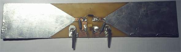
The indicator is a panel made of foiled PCB measuring 24x5cm. The circuit does not require just such a design solution - it is possible to use antennas "MUSTACHE", etc. The size of the antenna depends on the length of the measured wave.
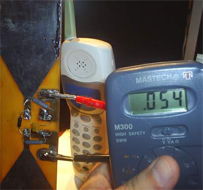
The measurements were carried out with an M300 multimeter in millivoltmeter mode. The main advantage is the wide measurement range. Starting from 0 to 5V.

Basically, measurements do not go beyond 200-300 mV. The photo shows measurements of the power supply (from a Wi-Fi access point) - voltage 1.1V. The maximum recorded value is very large - 4.5V, the magnetic field is quite high, but due to the low frequency of the field 15-20 cm from the device, the value is close to 0.
Searching for devices emitting high-frequency radiation, such as listening devices (bugs, microphones), is quite simple. The indicator easily and confidently determines the direction from which the radiation is coming. The source is detected from a distance of 3-5m, even if it is an ordinary cell phone. An increase in the instrument reading indicates that the search direction is correct. More often, on the upper floors of a house in an apartment there is an electromagnetic “background”. This electromagnetic field strength is apparently due to powerful radiation sources within a radius of several hundred meters: the bases of cellular operators.
The indicator does not have its own amplifier, so the result depends on which antenna design was chosen. Capacitor C1 is a reactance that “cuts” frequencies and allows you to configure the indicator to a certain range. Fine tuning was not carried out due to the lack of a reference frequency generator or a good frequency meter.
Solder tinning has been performed. This is not at all necessary. In principle, after etching the board, thorough washing and drying is required.
As an analogue that can be used instead of the D1 diode GD507A, I recommend using the KD922B with a maximum frequency of 1 GHz. In terms of characteristics at medium frequencies up to 400 MHz, KD922B is twice as superior to its germanium counterpart. Also, during test measurements from a 150 MHz radio station with a power of 5 W, 4.5 V of peak voltage was obtained with the GD507A, and with the help of the KD922B a power 3 times higher was obtained.
When measuring lower frequencies (27 MHz), no significant differences between the diodes are observed. The indicator is well suited for setting up transmission equipment and high-frequency generators. The indicator does not allow you to determine the frequency, distortion or harmonics of the transmitter, but I think nothing prevents you from modifying the circuit, amplifying the signal - connecting a receiver and an oscilloscope.
Electric field indicators can be used for individual protection of electricians when searching for faults in electrical networks. With their help, the presence of electrostatic charges in semiconductor, textile production, and storage of flammable liquids is determined. When searching for sources of magnetic fields, determining their configuration and studying the stray fields of transformers, chokes and electric motors, one cannot do without magnetic field indicators.
The circuit of the high-frequency radiation indicator is shown in Fig. 20.1. The signal from the antenna reaches a detector made of a germanium diode. Next, through an L-shaped LC filter, the signal enters the base of the transistor, in the collector circuit of which a microammeter is connected. It is used to determine the power of high-frequency radiation.
To indicate low-frequency electric fields, indicators with a field-effect transistor input stage are used (Fig. 20.2 - 20.7). The first of them (Fig. 20.2) is made on the basis of a multivibrator [VRYA 80-28, R 8/91-76]. The field-effect transistor channel is a controlled element, the resistance of which depends on the magnitude of the controlled electric field. An antenna is connected to the gate of the transistor. When the indicator is introduced into the electric field, the source-drain resistance of the field-effect transistor increases and the multivibrator turns on.
A sound signal is heard in the telephone capsule, the frequency of which depends on the strength of the electric field.


The following two designs according to the schemes of D. Bolotnik and D. Priymak (Fig. 20.3 and 20.4) are intended for troubleshooting New Year's electrical garlands [R 11/88-56]. The indicator (Fig. 20.3) is generally a resistor with controlled resistance. The role of such resistance is again played by the drain channel - the source of the field-effect transistor, supplemented by a two-stage DC amplifier. The indicator (Fig. 20.4) is made according to the circuit of a controlled low-frequency generator. It contains a threshold device, an amplifier and a detector of the signal induced in the antenna by an alternating electric field. All these functions are performed by one transistor - VT1. Transistors VT2 and VT3 are used to assemble a low-frequency generator operating in standby mode. As soon as the device's antenna is brought closer to the source of the electric field, transistor VT1 turns on the sound generator.


The electric field indicator (Fig. 20.5) is designed to search for hidden wiring, energized electrical circuits, indicate proximity to the area of high-voltage wires, the presence of alternating or constant electric fields [RaE 8/00-15].
The device uses a inhibited generator of light-sound pulses, made on an analogue of an injection-left-field transistor (VT2, VT3). In the absence of a high-intensity electric field, the drain-source resistance of field-effect transistor VT1 is small, transistor VT3 is closed, and there is no generation. The current consumed by the device is units or tens of μA. In the presence of a constant or alternating electric field of high intensity, the drain-source resistance of the field-effect transistor VT1 increases, and the device begins to produce light and sound signals. So, if the gate terminal of transistor VT1 is used as an antenna, the indicator reacts to the approach of the network wire at a distance of about 25 mm.
Potentiometer R3 adjusts the sensitivity, resistor R1 sets the duration of the light-sound message, capacitor C1 sets the frequency of their repetition, and C2 determines the timbre of the sound signal.
To increase sensitivity, a piece of insulated wire or a telescopic antenna can be used as an antenna. To protect transistor VT1 from breakdown, a zener diode or a high-resistance resistor should be connected parallel to the gate-source transition.
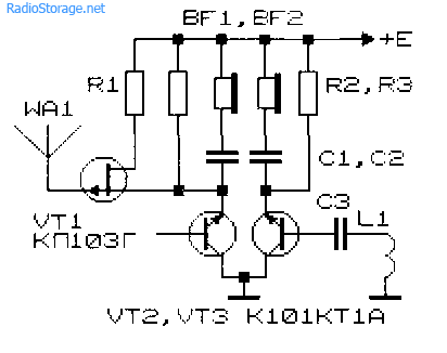
The indicator of electric and magnetic fields (Fig. 20.6) contains a relaxation pulse generator. It is made on a bipolar avalanche transistor (transistor of the K101KT1A microcircuit, controlled by an electronic switch on a field-effect transistor of the KP103G type), to the gate of which an antenna is connected. To set the operating point of the generator (generation failure in the absence of indicated electric fields), resistors R1 and R2 are used. The pulse generator is loaded through capacitor C1 onto high-impedance headphones. In the presence of an alternating electric field (or the movement of objects carrying electrostatic charges), an alternating current signal appears on the antenna and, accordingly, the gate of the field-effect transistor, which leads to a change in the electrical resistance of the drain-source junction with a modulation frequency. In accordance with this, the relaxation generator begins to generate packets of modulated pulses, and a sound signal will be heard in the headphones.
The sensitivity of the device (detection range of a current-carrying wire of a 220 V 50 Hz network) is 15...20 cm. A 300x3 mm steel pin is used as an antenna. With a supply voltage of 9 V, the current consumed by the indicator in silent mode is 100 μA, in operating mode - 20 μA.
The magnetic field indicator (Fig. 20.6) is made on the second transistor of the microcircuit. The load of the second generator is a high-impedance headset. The alternating current signal, taken from the inductive magnetic field sensor L1, is fed through the transition capacitor C1 to the base of the avalanche transistor, which is not connected via direct current to other elements of the circuit (“floating” operating point). In the alternating magnetic field indication mode, the voltage on the control electrode (base) of the avalanche transistor changes periodically, and the avalanche breakdown voltage of the collector junction and, in connection with this, the frequency and duration of generation also changes.

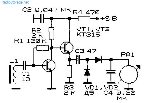
The indicator (Fig. 20.7) is made on the basis of a voltage divider, one of the elements of which is a field-effect transistor VT1, the resistance of the drain-source junction of which is determined by the potential of the control electrode (gate) with the antenna connected to it [Rk 6/00-19]. A relaxation pulse generator based on avalanche transistor VT2, operating in standby mode, is connected to the resistive voltage divider. The initial voltage level (operation threshold) supplied to the relaxation pulse generator is set by potentiometer R1.
To prevent breakdown of the control transition of the field-effect transistor, protection is introduced into the circuit (when the power source is turned off, the gate-source circuit is short-circuited). An increase in the volume level of the sound signal is achieved by introducing an amplifier using a bipolar transistor VT3. A low-resistance telephone capsule can be used as a load for the output transistor VT3.
To simplify the circuit, a high-resistance telephone capsule, for example, TON-1, TON-2 (or “medium-resistance” - TK-67, TM-2) can be included instead of resistor R3. In this case, there is no need to use elements VT3, R4, C2. The connector into which the telephone is plugged in can simultaneously serve as a power switch to reduce the size of the device.
In the absence of an input signal, the resistance of the drain-source transition of the field-effect transistor is several hundred Ohms, and the voltage removed from the potentiometer slide to power the relaxation pulse generator is small. When a signal appears at the control electrode of the field-effect transistor, the resistance of the drain-source junction of the latter increases in proportion to the level of the input signal to units or hundreds of kOhms. This leads to an increase in the voltage supplied to the relaxation pulse generator to a value sufficient to produce oscillations, the frequency of which is determined by the product R4C1. The current consumed by the device in the absence of a signal is 0.6 mA, in indication mode - 0.2...0.3 mA. The detection range of a current-carrying wire of a 220 V 50 Hz network with a whip antenna length of 10 cm is 10...100 cm.

The high-frequency electric field indicator (Fig. 20.8) [MK 2/86-13] differs from its analogue (Fig. 20.1) in that its output part is made according to a bridge circuit, which has increased sensitivity. Resistor R1 is designed to balance the circuit (set the instrument needle to zero).
The standby multivibrator (Fig. 20.9) is used to indicate the mains voltage [MK 7/88-12]. The indicator operates when its antenna approaches the network wire (220 V) at a distance of 2...3 cm. The generation frequency for the ratings shown in the diagram is close to 1 Hz.

Indicators of magnetic fields according to the diagrams presented in Fig. 20.10 - 20.13, have inductive sensors, which can be a telephone capsule without a membrane, or a multi-turn inductor with an iron core.
The indicator (Fig. 20.10) is made according to the 2-V-0 radio receiver circuit. It contains a sensor, a two-stage amplifier, a voltage doubling detector and an indicating device.
Indicators (Fig. 20.11, 20.12) have LED indication and are designed for high-quality indication of magnetic fields [R 8/91-83; R 3/85-49].


The indicator according to the I.P. scheme has a more complex design. Shelestov, shown in Fig. 20.13. The magnetic field sensor is connected to the control junction of a field-effect transistor, the source circuit of which includes load resistance R1. The signal from this resistance is amplified by a cascade on transistor VT2. Further, the circuit uses a comparator on a DA1 chip of the K554СAZ type. The comparator compares the levels of two signals: the voltage taken from the adjustable resistive divider R4, R5 (sensitivity regulator) and the voltage taken from the collector of transistor VT2. The LED indicator is turned on at the comparator output.
Literature: Shustov M.A. Practical circuit design (Book 1), 2003